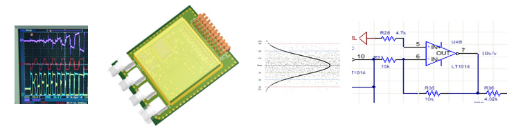


Sensor Interfacing AFE’s
Sensors generally require careful attention to the analog design. As sensors get more sensitive, the signal to noise ratio becomes a challenge. Bench testing and simulation are basic tools used to create a robust analog front end. System interfacing is integrated into the design as well ensuring a clean signal chain. For really low noise, the ADC is located as close to the sensor as possible with careful attention to printed circuit board layout for shielding and reliability from device to device. Grounding is often overlooked by some engineers but is a common root cause for noisy signals. Environmental factors such as an electrically noisy environment in a SMPS can often require a dedicated isolated supply and fully shielded signal traces. More subtle things like frequency response, impedance matching, input bias currents, all contribute to good (or bad) signal fidelity. Getting the sub-circuit to a small demonstration device is key to exception performance in the final design.Generalized Design Procedure
1. Sensor Characterization (model, bench, and environmental testing)
2. Signal Capture
3. Circuit Simulation
4. Mini Prototype and test
5. Verify on multiple Sensors/PCB’s
The benefits to this step is a small development effort prior to developing full solution PCB